
- Home
- Laser marking
- Fiber laser marking series
- Automated Laser De-Molding System for Reclaimed Wafers
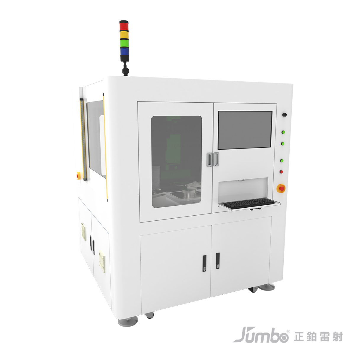
Automated Laser De-Molding System for Reclaimed Wafers
-
Supports Reclaimed Wafer Processing:
The equipment is suitable for wafer grinding and cleaning processes, enabling the reuse of wafers that do not meet IC manufacturing standards or are used as dummy/control wafers. This helps reduce testing costs and improve resource utilization. -
Reduces Environmental Impact:
Wastewater generated during the grinding process—containing silicon particles and chemical substances—can be managed with wastewater treatment modules, minimizing potential environmental harm. -
Meets High-Demand Application Fields:
Reclaimed wafers are ideal for process development in industries such as solar energy and silicon-based semiconductors, fulfilling testing and monitoring requirements while enhancing overall process efficiency. -
Built-in Laser Micromachining Module:
Equipped with high-precision laser marking capabilities, the equipment can directly mark serial numbers, QR codes, and other production traceability data on wafers, ensuring accurate and reliable identification. -
Complies with Semiconductor Process Standards:
The laser marking technology offers high durability and resistance to harsh processing conditions, making it especially suitable for high-standard environments such as packaging and testing stages.
-
Product number
-
JBL-LMF
-
-
Application Introduction
-
Widely used in industries requiring high precision and reliability, such as electronics, automotive (e.g., EV motor copper welding), medical devices, and aerospace.
-
-
-
Equipment Specifications
-
Laser source power :800W
Processing range :40*40mm
Work Environment :10~45℃ , <70%
power supply :3kw / AC220V
Cooling method :Water Cooling
Equipment weight : 800kg
Equipment size :1300*1500*1800mm -
-


